
The next breakthrough in technology may not be another advancement in software, but may hinge on the literal angle between materials. Certain quantum effects arise when one atom-thick materials are stacked on top of each other with a slight twist (or, less commonly, with a small lattice mismatch or atomic alignment shift). These misaligned, layered materials, called moiré materials or devices, give rise to highly sought-after quantum properties, and could lead to technological devices with enhanced speed, efficiency, and robustness.
- - - - - - - - - - - - - - - - - - - - - - - - - - - - - - - - - - - - - - - - - - - - - - - - - - - - - - - - - - - - - - - - - - -
Understanding the origin of quantum properties requires understanding the behavior of electrons. The structure of an atom is a positively charged nucleus surrounded by a cloud of negatively charged electrons, held together by the attractive force between the two. The position of electrons isn’t described with a single definite value, but rather with a probability. In a crystal lattice or any repeating structure, the arrangement of atoms forms a periodic potential: essentially a landscape that strongly influences where the electron can be.
With this in mind, imagine a moiré device as layers of atomically thin, patterned mesh screens. The periodic potential has very low values in the gaps between atoms.
When these meshes are laid atop each other with a slight twist, it creates a large-scale “super pattern” called the moiré pattern or superlattice, which forms pockets within the layers that can quasi-localize (somewhat localize) electrons and holes – a conceptual way to describe the absence of an electron in a material. 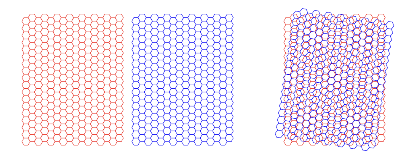
Understanding the state of electrons and holes within a material is crucial because their energy levels and interactions govern key electronic behaviors—such as electrical conductivity, magnetic ordering, and the emergence of topological phases. The quasi-localization amplifies the interactions between electrons and holes, leading to unique quantum phases. One such example, among many, is unconventional superconductivity, which occurs when the strong interactions between electron pairs allow them to flow with little resistance.
- - - - - - - - - - - - - - - - - - - - - - - - - - - - - - - - - - - - - - - - - - - - - - - - - - - - - - - - - - - - - - - - - - -
This is, of course, a wild simplification of these devices, and with their complexity also comes many roadblocks in the field. One major challenge is that these devices are still handmade by researchers. This limits usable device area to a few square micrometers, as well as presenting an issue of human error and deviation during mechanical exfoliation of materials and assembly. Atoms also tend to shift to make the most stable arrangement, resulting in strain within the twisted device, altering the moiré pattern, and impacting the device’s properties. Additionally, accurately modelling the complex interactions between the thousands of atoms and particles within a device is still a massive challenge for theory and simulation.
However, rapid progress is already being made to tackle these issues. Although moire devices were initially constructed with twisted bilayers of graphene, over the past few years, researchers have investigated the use of other materials. Specifically, transition metal dichalcogenides (TMDs), materials formed from the bonding of transition metals and chalcogenides (an element group). TMD-based moirés offer more robust devices and additional controllability over device effects.
If these hurdles are cleared, moiré devices could shift from curiosity to highly configurable materials for next‑generation electronics.
Citations:
Mak, K. F., & Shan, J. (2022). Semiconductor moiré materials. Nature Nanotechnology, 17,
686–695. https://doi.org/10.1038/s41565-022-01165-6
Chubarov, M., Choudhury, T. H., Reifsnyder Hickey, D., Bachu, S., Zhang, T., Sebastian, A.,
Bansal, A., Zhu, H., Trainor, N., Das, S., Terrones, M., Alem, N., & Redwing, J. M. (2021). Wafer-scale epitaxial growth of unidirectional WS2 monolayers on sapphire. ACS Nano, 15(2), 2532–2541. https://doi.org/10.1021/acsnano.0c06750
Zheng, H., Wu, B., Li, S., Ding, J., He, J., Liu, Z., Wang, C.-T., Wang, J.-T., Pan, A., & Liu, Y.
(2023). Localization-enhanced moiré exciton in twisted transition metal dichalcogenide
heterotrilayer superlattices. Light: Science & Applications, 12, 117.
https://doi.org/10.1038/s41377-023-01171-w
Lee, S. (2025, June 10). Unconventional superconductors: A deep dive. Number Analytics.
https://www.numberanalytics.com/blog/unconventional-superconductors-guide